If you’ve been watching the CPU space, you’ve seen the rapid descent from 7nm to 5nm, and now down to 3nm and even 2nm. It feels like Moore’s Law is alive and well, at least for logic. But then you look at the RAM specs on a new smartphone or server, and you see something that looks like a relic from a decade ago: “10nm-class.” It feels stagnant. It feels like the industry stopped trying. The reality is far more complex—and far more expensive for you as a consumer.
The stagnation isn’t an accident; it’s a fundamental physical barrier. While manufacturers like SK Hynix, Samsung, and Micron throw around terms like “1c” or “1d” nodes, they are playing a linguistic game to hide the fact that memory cells simply do not scale like the transistors on your processor. This isn’t just a war of specs on a sheet; it’s a supply chain squeeze that is about to hit your wallet hard, driven by an AI boom that is gobbling up every bit of memory capacity available.
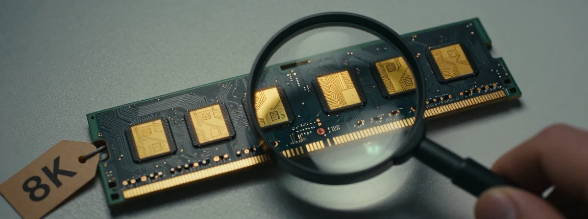
You need to understand that when a memory maker says “10nm,” they aren’t measuring the same thing as when a CPU maker says “3nm.” The numbers are marketing labels, designed to make you feel like progress is happening linearly. But under the microscope, the physics tells a different story—one where shrinking the cell further destroys the data it’s supposed to store.
Why DRAM Hit a Wall a Decade Ago
We have been stuck in the 10nm to 20nm range for DRAM for roughly ten years. To understand why, you have to look at how a DRAM cell is built versus a logic transistor. A CPU transistor is essentially a switch—it either allows current to flow or it doesn’t. Shrink it down, and you get more switches per square inch, and generally, they consume less power. It’s difficult, but the physics rewards the effort.
A DRAM cell is different. It consists of a capacitor and a transistor acting as a gate. The capacitor stores electrons to represent a bit. To work reliably, that capacitor needs to hold a specific amount of charge. If you shrink the cell too much, the capacitor becomes too small to hold enough electrons to distinguish a “1” from a “0” over a sustained period. Leakage currents become a nightmare. If you try to force DRAM into the 2nm nodes used for CPUs, you don’t get high-density memory; you get a useless chip that forgets its data the moment you look away.
This is why the industry has shifted to “1c” or “1d” class nodes rather than honest nanometer measurements. When you see a “10nm-class” label, particularly a “1c” level node, it usually translates to roughly 12nm in reality. And by 12nm, I mean whatever the manufacturer calculates they can get away with while selling you a product. It is a defined term that exists largely to keep the roadmap looking active, even as the physical shrinking slows to a crawl.
The “2nm” Expectation vs. Reality
There is a persistent misconception that because logic chips are hitting 2nm, memory should follow suit. It’s a reasonable assumption if you don’t know the physics, but it leads to disappointment. Memory logic made on 2nm nodes will not be significantly denser than what we have now at 10nm. We cannot shrink them down without them becoming unreliable and thus useless.
The industry has hit a point of diminishing returns. We can tweak the aspect ratios, bury wordlines deeper, and use high-K dielectrics to squeeze out a few percentage points of efficiency, but we cannot break the laws of physics. The capacitor is the bottleneck. You can make the transistor smaller, but if the capacitor can’t hold the charge, the cell fails. This is why you don’t see 2nm DRAM, and why you won’t see it anytime soon. The marketing terms will continue to evolve—“10nm Class 6” or similar—but the actual density improvements are becoming incremental, not exponential.
This has massive implications for performance. The only way to get more bandwidth now isn’t just by shrinking the cell to pack more in, but by making the interface faster and wider. We are seeing efficiency gains and higher bandwidth with these newer “10nm-class” generations, which will make the next generation of smartphones noticeably snappier. But don’t confuse that speed with a massive leap in density or a drop in manufacturing cost. The physics of the capacitor is a hard ceiling.
The AI Tax on Your Hardware
If memory scaling is stalling, why are prices going up? You can thank the artificial intelligence boom. There is a massive RAM shortage right now, and it is not because of smartphone users. It is because Google, Microsoft, and Amazon are hoarding every bit of high-bandwidth memory they can get their hands on to train and run massive LLMs.
The money has flowed toward the hyperscalers. When data centers are willing to pay a premium for HBM (High Bandwidth Memory) and standard DDR5 modules to keep their AI clusters running, the manufacturers prioritize that capacity. This leaves the consumer market—your phones, laptops, and tablets—scrambling for scraps. This dynamic drives up pricing for everyone. Even Apple, with their massive supply chain leverage and vertical integration, might be able to shield their customers longer than most, but the tide raises all boats eventually.
You are effectively competing with a supercomputer cluster for the same silicon wafers. When you hear about “mass production” of new memory nodes, remember that the first batches aren’t going into a flagship phone; they are going into a server rack. This supply crunch is the real reason your next device upgrade is going to cost more, not because the “10nm” label suddenly became more premium.
Decoding the Marketing Labels
So, how do you read between the lines? When you see a spec sheet boasting about a “1c” or “10nm-class 6” node, recognize it for what it is: a measure of efficiency, not raw size. These nodes represent the fourth or fifth generation of tweaks to a roughly 12nm geometry. They bring genuine benefits—lower power consumption and higher data rates are critical for battery life and app responsiveness.
But be skeptical of density claims. A “10nm” DRAM chip today is not twice as dense as a “20nm” chip from years ago. The scaling curve has flattened. The manufacturers are doing incredible work to keep progress moving through architectural changes rather than just shrinking features, but it is a much harder, more expensive road.
The “nm” label is mostly a marketing term anyways, defined differently for CPUs and GPUs than for memory cells. In logic, it refers to gate length or metal pitch. In memory, it’s a loose approximation of the effective cell size. Comparing the two directly is like comparing the fuel efficiency of a jet to a scooter based on their engine RPM. It’s a category error that marketing teams are happy to let you make.
The Real Cost of Progress
We are entering an era where the cheap, abundant scaling of the past is over. Memory manufacturers are fighting physics to squeeze out every last electron of efficiency, and that fight costs money. Simultaneously, the insatiable demand from AI data centers is tightening supply. The result is a market where you get better performance and efficiency, but not necessarily better value in terms of dollars-per-gigabyte.
The next generation of smartphones will be faster. “10nm Class 6” technology means more efficiency and higher bandwidth, which you will feel in speed and battery life. That part is true. But the idea that we are on a steady march to 2nm memory is a fantasy. We are optimizing the heck out of a mature technology, and you are going to pay a premium for those optimizations.
Look past the node names. Focus on the actual bandwidth and power efficiency numbers. Those are the specs that translate to real-world performance. And be prepared for higher prices—the days of cheap, exponentially scaling memory are likely behind us.